用户测试程序
设计一个用户测试程序,首先打开 /dev/pio_button设备节点,触发驱动中的 open函数,注册中断,然后在死循环中调用 read 阻塞等待按键事件,每次 read返回后,解析 button_val的2个bit位,打印被按下的按键编号。
button_test.c 源码如下:
#include <stdio.h>
#include <sys/types.h>
#include <sys/stat.h>
#include <fcntl.h>
#include <unistd.h>


int main(int argc ,char *argv[])
{
    int fd;
    unsigned char button_val;
    int i;
    unsigned char mask=0x01;
    fd = open("/dev/pio_button",O_RDWR);
    if (fd < 0)
    {
        printf("open file error\n");
    }
    while(1)
    {
        mask=0x01;
        read(fd,&button_val,1);
        for(i=0;i<2;i++)
        {
            if(button_val&mask)
                 printf("button[%d] is pressed\n",i);
            mask<<=1;
        }
    }
    return 0;
}
执行如下命令生成应用程序可执行文件button_test:
aarch64-linux-gnu-gcc -o button_test button_test.c 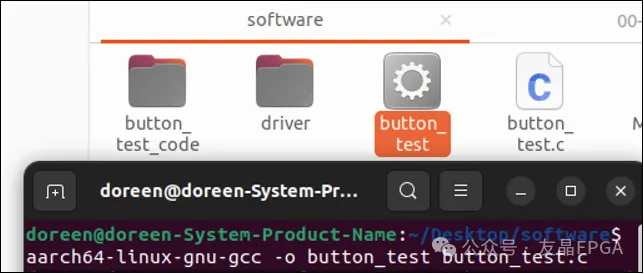
下板测试
前面已经按照Agilex 5 SOC FPGA的HPS端如何响应FPGA端中断——修改Quartus工程(GHRD工程) 将FPGA配置文件固化到QSPI FLASH里面去了。
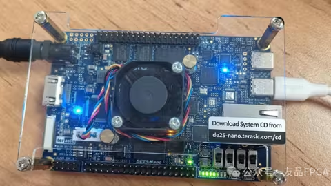
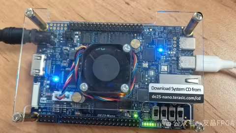
按照友晶教程【教程】Linux上用命令烧写SD卡和Windows上用Win32DiskImager工具一键烧写SD卡 将de25_nano_revA_sdcard_console_v1.1.img 烧写到SD卡。
按照友晶教程【教程】Linux上用命令烧写SD卡和Windows上用Win32DiskImager工具一键烧写SD卡 打开串口,然后启动开发板linux系统。
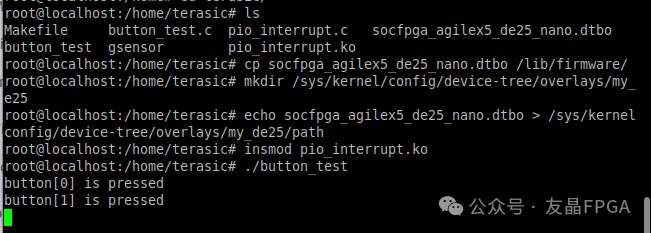
按顺序执行如下命令:
sudo su

cp socfpga_agilex5 de25_nano.dtbo /lib/firmware/

mkdir /sys/kernal/config/device-tree/overlays/my_de25

ehco socfpga_agilex5 de25_nano.dtbo > /sys/kernal/config/device-tree/overlays/my_de25/path

insmod pio_button.ko

./button_test
分别按KEY0 和KEY1会打印button[0] is pressed 和button[l] is pressed,如下图:
本文源码参考:
https://github.com/hbwangjinwu/PIO_Interrupt/tree/master
结束语
本教程完整介绍了在DE25-Nano平台上实现HPS响应FPGA端中断的完整流程——从硬件设计、设备树配置、平台驱动开发到用户态测试程序。通过PIO按键中断实验,读者可以掌握SoC FPGA异构平台中FPGA与HPS之间中断交互的核心技术,为更复杂的嵌入式系统开发奠定基础。该驱动框架同样适用于其他FPGA端外设(如ADC、自定义IP核等)的中断处理场景。
文章来源:友晶科技