注:本文转载自: https://blog.csdn.net/botao_li/article/details/85257566
本文档及此文档系列中使用zcu102开发板的全部文档均使用以下开发环境:
本文首先说明了PL开发的完整流程,再对仿真和调试功能进行单独说明。
本文所用Vivado工程见 https://download.csdn.net/download/botao_li/10877016
建立工程
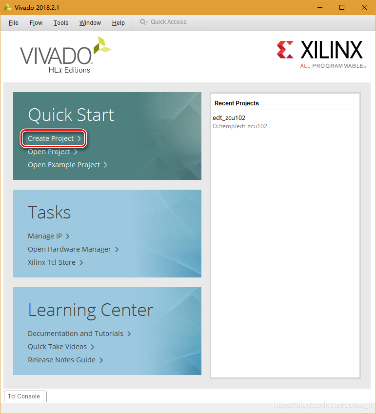
启动Vivado,选择Create Project
进入新建工程向导
在Project Name页设置工程名称及路径

在Project Type页选择RTL Project,并且选中Do not specify sources at this time

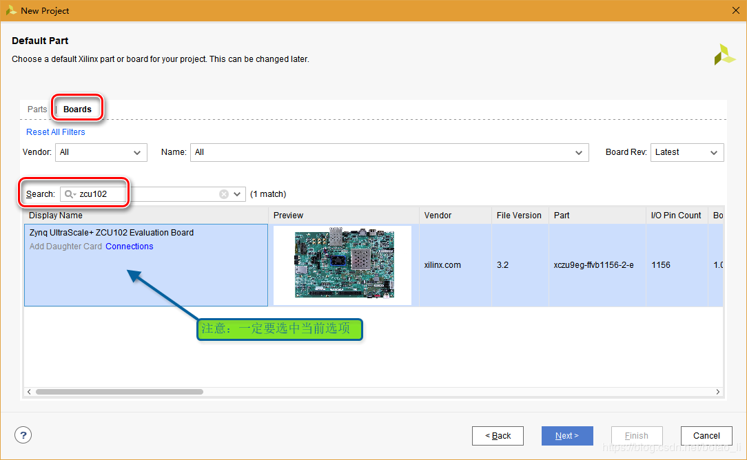
在Default Part页选择zcu102开发板
完成后点击Finish,建立工程完毕
添加时钟
根据ug1182 zcu102 evaluation board user guide,当前工程使用板上125MHz固定频率差分时钟。
由于管脚所在Bank为HIGH_DENSITY IO Bank,不能使用PLL或者MMCM等时钟模块,因此先由IBUFDS转化为单端时钟后直接使用。IBUFDS调用代码见添加设计文件部分的代码。
添加设计文件
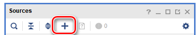
在Sources窗口选择Add Sources
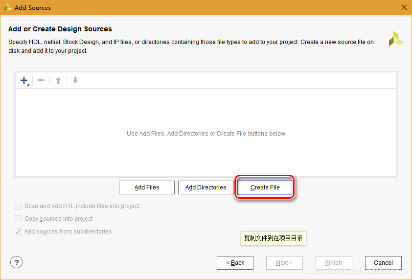
在弹出的Add Sources窗口,选择Add or create design sources

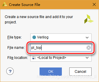
在Add or Create Design Sources页选择Create File
在弹出窗口中输入文件名称
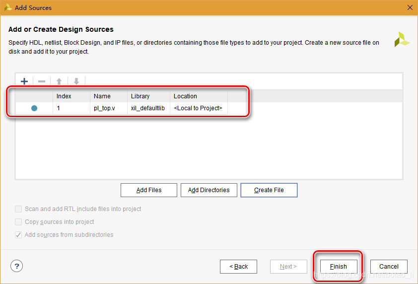
回到Add Sources窗口点击Finish
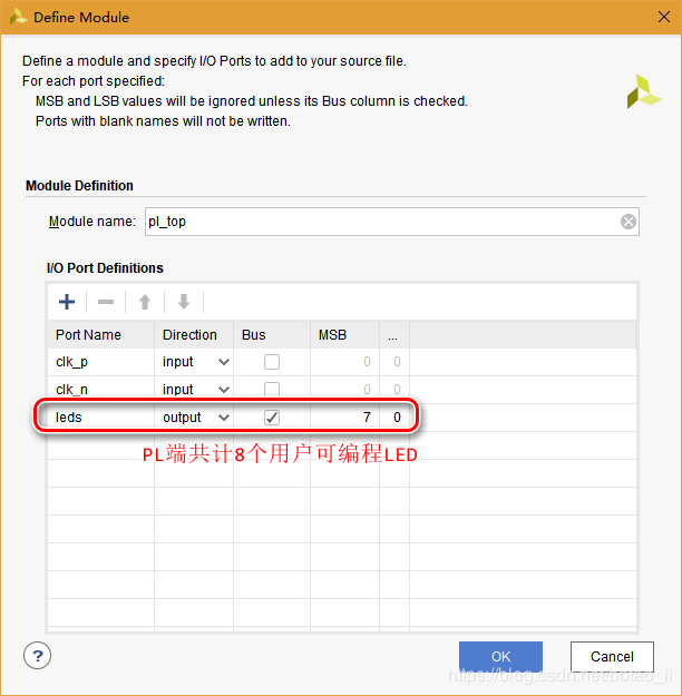
弹出的Define Module窗口中设置模块的输入输出端口,并选择OK
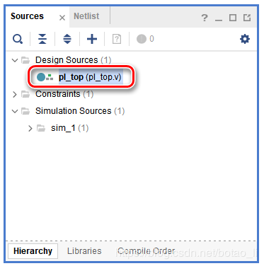
在Sources窗口双击新建的模块,编辑代码
打开代码后可以看到前述流程中自动添加的端口定义
module pl_top(
input clk_p,
input clk_n,
output [7:0] leds
);
endmodule
完成代码如下:
module pl_top(
input clk_p,
input clk_n,
output [7:0] leds
);
wire clk;//125MHz工作时钟
//用原语实现差分时钟转单端
IBUFDS
#(
.IOSTANDARD("DEFAULT")//DEFAULT默认所有情况
)
IBUFDS_inst
(
.O(clk),//输出
.I(clk_p),//P端输入
.IB(clk_n)//N端输入
);
//定义输出寄存器
reg [7:0] leds = 8'b0000_0001;
//计数器,计时1秒,计数范围0~27'd125_000_000-1
reg [26:0] cnt = 27'd0;
always @(posedge clk) begin
case (cnt)
27'd124_999_999: begin
cnt <= 27'd0;//计数复位
leds <= {leds[6:0], leds[7]};//循环移位
end
default: begin
cnt <= cnt+27'd1;//计数
leds <= leds;//保持
end
endcase
end
endmodule
添加约束文件
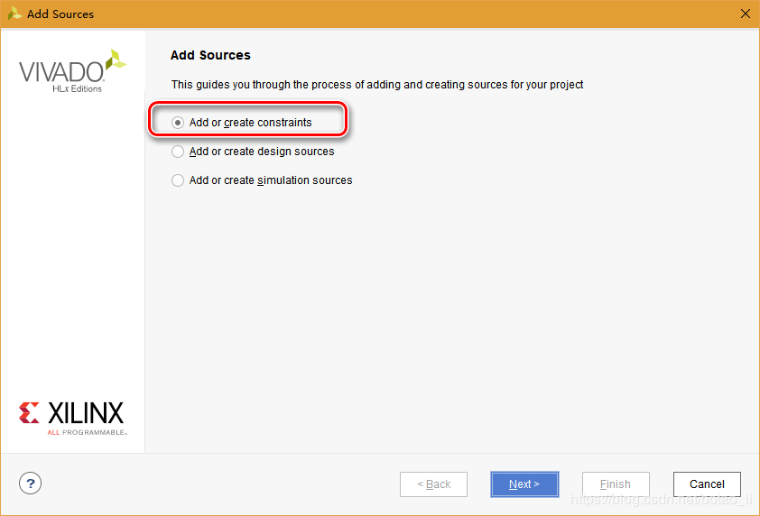
使用与前述相同的方法打开Add Sources窗口,选择Add or create constraints
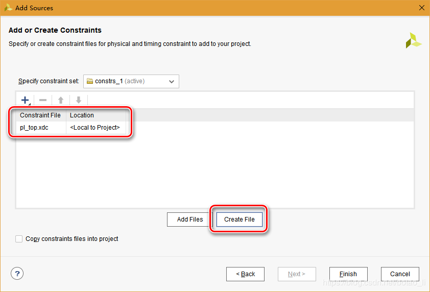
选择Create File,建立xdc约束文件,点击Finish完成
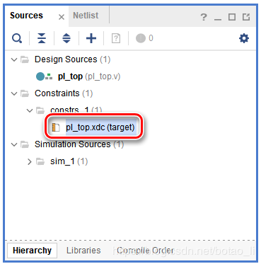
在Sources窗口可以看到新建立的约束文件
综合
在SYNTHESIS选择Run Synthesis

弹出窗口按默认设置选择OK开始综合
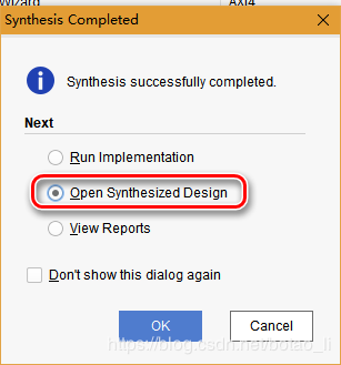
综合结束后在弹出窗口选择Open Synthesized Design(或者在Flow Navigator的SYHTHESIS项下选择)
添加管脚约束
在Layout菜单选择I/O Planning

在I/O Ports页设置所有顶层管脚的Package Pin和I/O Std(参考ug1182)

选择保存弹出Out of Date Design,选择OK
接下来弹出的Save Constraints窗口中指定前述建立的xdc约束文件
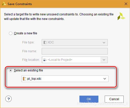
在Sources窗口双击打开pl_top.xdc文件可以看到保存的管脚约束代码
set_property PACKAGE_PIN AL12 [get_ports {leds[7]}]
set_property PACKAGE_PIN AH14 [get_ports {leds[6]}]
set_property PACKAGE_PIN AH13 [get_ports {leds[5]}]
set_property PACKAGE_PIN AJ15 [get_ports {leds[4]}]
set_property PACKAGE_PIN AJ14 [get_ports {leds[3]}]
set_property PACKAGE_PIN AE13 [get_ports {leds[2]}]
set_property PACKAGE_PIN AF13 [get_ports {leds[1]}]
set_property PACKAGE_PIN AG14 [get_ports {leds[0]}]
set_property IOSTANDARD LVCMOS33 [get_ports {leds[7]}]
set_property IOSTANDARD LVCMOS33 [get_ports {leds[6]}]
set_property IOSTANDARD LVCMOS33 [get_ports {leds[5]}]
set_property IOSTANDARD LVCMOS33 [get_ports {leds[4]}]
set_property IOSTANDARD LVCMOS33 [get_ports {leds[3]}]
set_property IOSTANDARD LVCMOS33 [get_ports {leds[2]}]
set_property IOSTANDARD LVCMOS33 [get_ports {leds[1]}]
set_property IOSTANDARD LVCMOS33 [get_ports {leds[0]}]
set_property PACKAGE_PIN G21 [get_ports clk_p]
set_property IOSTANDARD LVDS_25 [get_ports clk_p]
set_property IOSTANDARD LVDS_25 [get_ports clk_n]
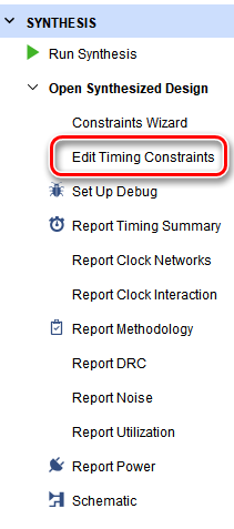
添加时钟约束
在SYNTHESIS选择Edit Timing Constraints
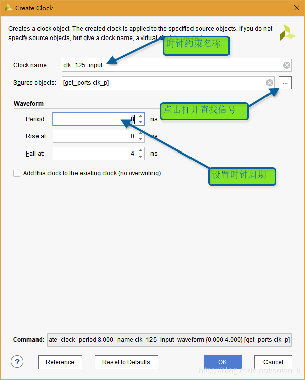
打开Timing Constraints页

双击Double click to create a Create Clock Constraint提示
在Create Clock窗口查找时钟并设置时钟周期

在Timing Constraints页面出现新建的时钟约束
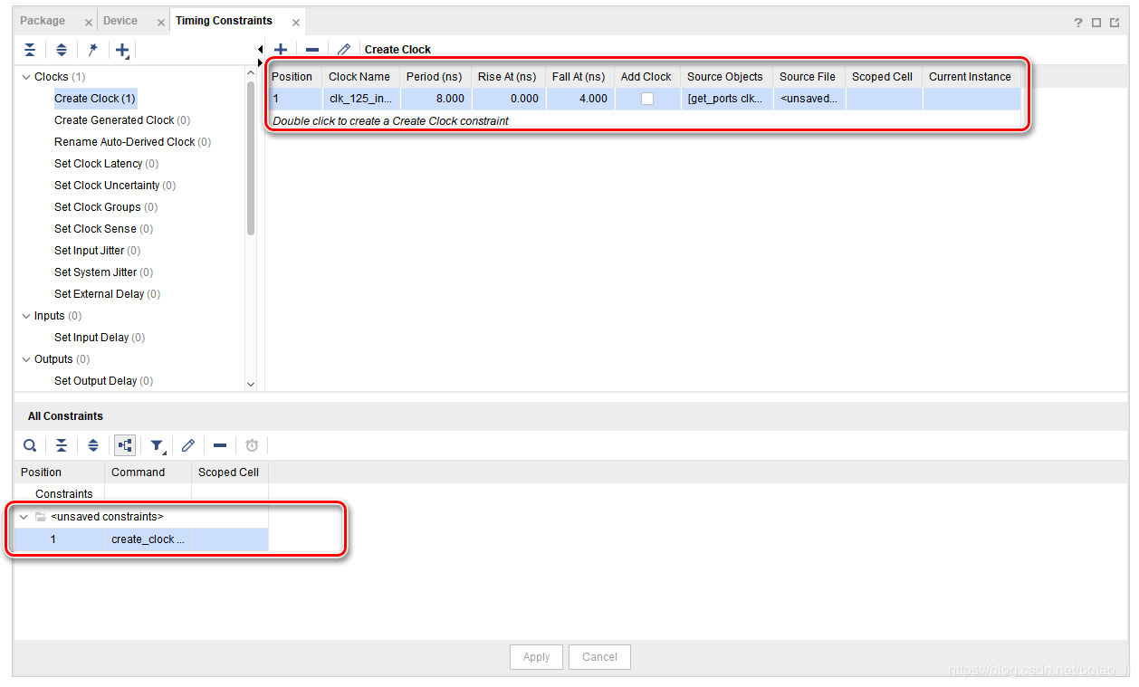
保存后在pl_top.xdc文件内出现时钟约束代码
create_clock -period 8.000 -name clk_125_input -waveform {0.000 4.000} [get_ports clk_p]
实现
在IMPLEMENTATION选择Run Implementation

弹出窗口按默认设置选择OK开始实现
结束后的弹出窗口中选择Open Implemented Design(或者在Flow Navigator的IMPLEMENTATION项下选择)
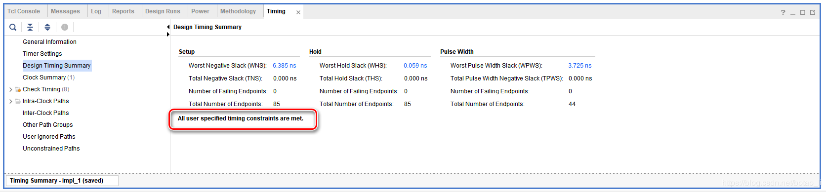
在Timing页,可以看到时钟约束全部通过
生成并烧写
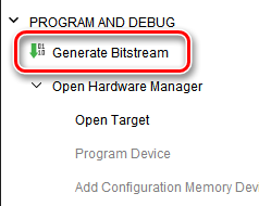
在PROGRAM AND DEBUG下点击Generate Bitstream
根据xtp435 zcu102 software install and board setup的说明,连接JTAG USB口,并且设置为JTAG加载之后,板卡上电
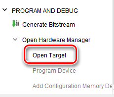
在PROGRAM AND DEBUG的Open Hardware Manager内选择Open Target
弹出菜单内选择Auto Connect
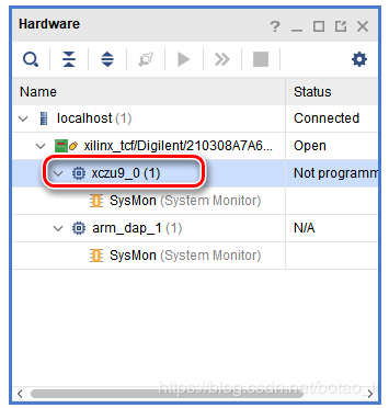
进入HARDWARE MANAGER界面后,在Hardware窗口选择xczu9_0器件,右键单击选择Program Device
在弹出的Program Device窗口选择生成的bit文件,并点击Program按钮

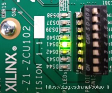
完成烧写后,板上LED按照代码设计依次点亮
仿真
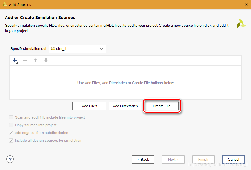
在Sources窗口选择Add Sources

在Add Sources窗口选择Add or create simulation sources

在下个步骤选择Create File
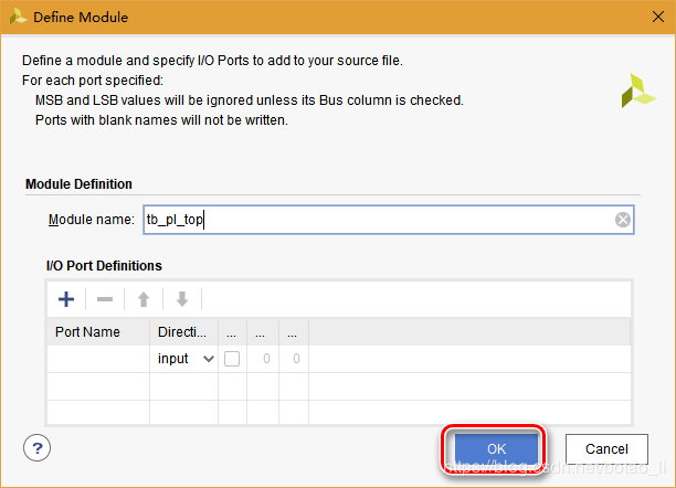
在Create Source File窗口设置文件名

完成后点击Finish按钮
之后弹出的Define Module窗口用于指定模块端口,由于是仿真激励,直接点击OK
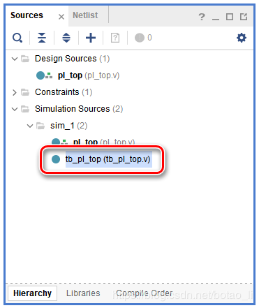
在Sources窗口找到新建的仿真模块,双击打开
修改后的仿真代码如下:
module tb_pl_top(
);
//建立差分时钟
reg clk_p = 1'b0;
wire clk_n;
assign clk_n = ~clk_p;
//设置时钟周期为8ns
always #4 clk_p = ~clk_p;
//定义led输出
wire [7:0] leds;
//例化
pl_top u
(
.clk_p(clk_p),
.clk_n(clk_n),
.leds(leds)
);
endmodule
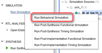
在Flow Navigator的SIMULATION中选择Run Simulation,在弹出菜单中选择Run Behavioral Simulation
之后进入SIMULATION界面
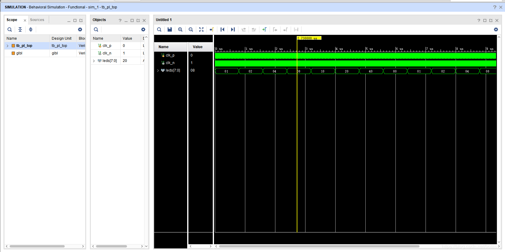
上方仿真波形是在修改设计代码中的计时长度后得到,否则仿真时间太长。
调试
此处的调试指上板调试,在FPGA运行中查看内部信号。
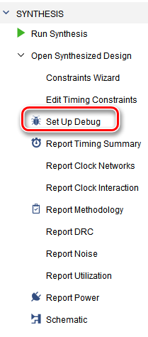
在SYNTHESIS下首先选择Open Synthesized Design,再选择Set Up Debug
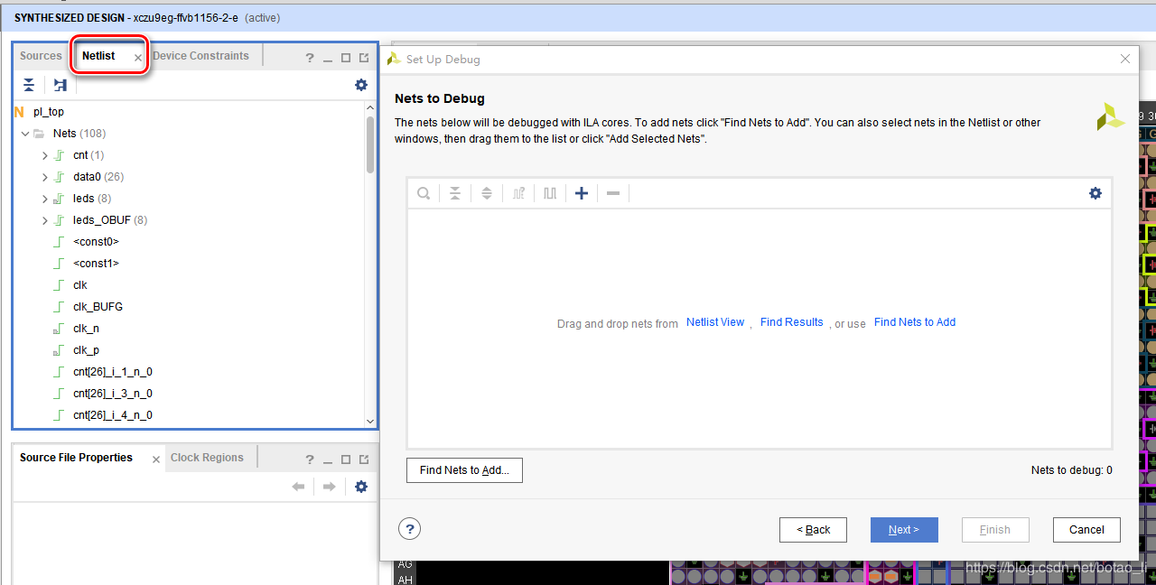
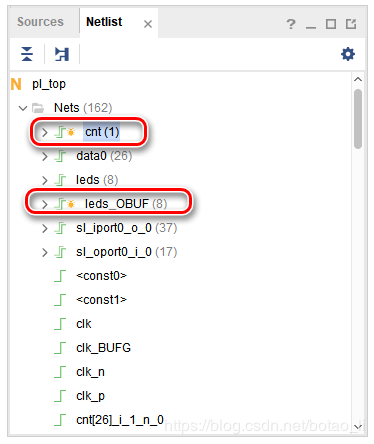
在弹出的Set Up Debug窗口中添加信号,简单的方法是从Netlist窗口直接拖入
若关注的信号没有在Netlist中出现,则可以在代码中信号定义之前添加 (* keep=“true” *)原语
(*keep="true"*) reg [26:0] cnt = 27'd0;

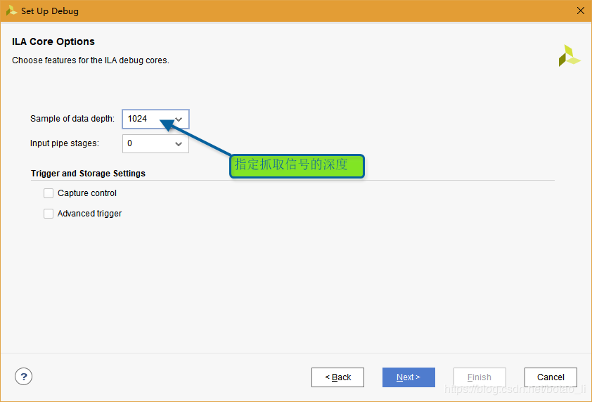
下一步骤中指定抓取信号的深度
之后点击Finish完成设置
在Netlist窗口可以发现添加的调试信号左侧出现了调试标记
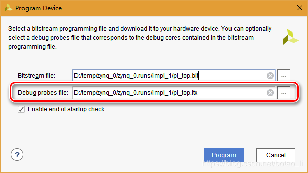
根据前述的说明重新生成bit文件后,打开烧写界面,在Program Device窗口可以发现自动添加的Debug文件
点击Program烧写完成后自动打开调试界面
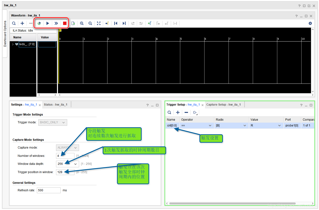
抓取结果:
