作者:Hello-FPGA,本文转载自:博客园
什么是Tandem PROM?
简单总结:市面多数的FPGA都是SRAM型,需要在上电时从外部存储器件完成代码的加载,对于具有PCIe功能的SRAM FPGA而言,必须要能够在规定的100ms(PCIe Spec规定,实际上多数计算机要求不会这么严格)时间内完成固件的加载,此时计算机才能够正确的枚举PCIe设备并分配对应的地址。100ms的时间对SPI FLASH而言是个很大的挑战,尤其是在FPGA SIZE越来越大时,为了解决这个问题,Xilinx为自己家的FPGA设备提出了Tandem Configuration的概念,核心思想是将FPGA固件分成2个部分,第一部分是PCIe部分,只负责PCIe的正常枚举,第二部分为用户逻辑。显然,这个技术需要FPGA厂商的支持,因此本文的Tandem专指Xilinx。
"PCI Express is a plug-and-play protocol meaning that at power up, the PCIe Host will enumerate the system. This process consists of the host reading the requested address size from each device and then assigning a base address to the device. As such, PCIe interfaces must be ready when the host queries them or they will not get assigned a base address. The PCI Express specification states that PERST# must deassert 100 ms after the power good of the systems has occurred, and a PCI Express port must be ready to link train no more than 20 ms after PERST# has deasserted. This is commonly referred to as the 100 ms boot time requirement. "
Tandem 有几种方式?
实际使用中,Tandem PROM最为简单,Tandem PCIe由于允许通过PCIe进行重配置,因此在服务器领域最为常用(在其它需要经常更新固件的场景下也适用)。本文只介绍Tandem PROM方式。
Tandem Configuration utilizes a two-stage methodology that enables the IP to meet the configuration time requirements indicated in the PCI Express specification. Multiple use cases are supported with this technology:
Tandem PROM: Load the single two-stage bitstream from the flash.
Tandem PCIe: Load the first stage bitstream from flash, and deliver the second stage bitstream over the PCIe link to the MCAP.
Tandem with Field Updates: After a Tandem PROM or Tandem PCIe initial configuration, update the entire user design while the PCIe link remains active. The update region (floorplan) and design structure are predefined, and Tcl scripts are provided.
Tandem + Partial Reconfiguration: This is a more general case of Tandem Configuration followed by Partial Reconfiguration (PR) of any size or number of PR regions.
Partial Reconfiguration over PCIe: This is a standard configuration followed by PR, using the PCIe / MCAP as the delivery path of partial bitstreams.
如何实现Tandem PROM?
本文介绍使用XDMA实现:
在xdma配置时选择advance mode,并选择Tandem模式;

然后右键选择生成example_design,根据打开的example_design配置,合理约束多出来的管脚,比如startup等interface;
根据example的约束进行修改、适配,下面给出SPI配置的示例;
--# --------------constraints-------------------- #
set_property BITSTREAM.GENERAL.COMPRESS TRUE [current_design]
set_property BITSTREAM.CONFIG.CONFIGFALLBACK Enable [current_design]
--#Expecting type 'enum' with possible values of '3,6,9,12,22,33,40,50,57,69,82,87,90,110,115,130,148'.
set_property BITSTREAM.CONFIG.CONFIGRATE 90 [current_design]
set_property CONFIG_VOLTAGE 3.3 [current_design]
set_property CONFIG_MODE SPIx4 [current_design]
set_property CFGBVS VCCO [current_design]
set_property BITSTREAM.CONFIG.SPI_BUSWIDTH 4 [current_design]
set_property BITSTREAM.CONFIG.UNUSEDPIN Pulldown [current_design]
set_property HD.TANDEM_IP_PBLOCK Stage1_Config_IO [get_cells sys_rst_n_IBUF_inst]
set_property HD.TANDEM_IP_PBLOCK Stage1_Main [get_cells test_i/util_ds_buf]
需要注意的地方有哪些?
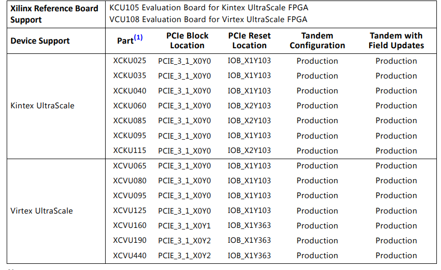
Tandem技术只在Xilinx较新的器件中支持

mcap_design_switch 这个信号非常有用,可以用作用户第二阶段逻辑的全局复位信号;
关于sys_reset复位信号
sys_reset 复位信号最好布局到BANK65,且用户自定义IO最好不要放置在BANK65,否则在约束时会引入很多的麻烦;