作者:OpenS_Lee
1背景知识
在我们的FPGA设计项目中,硬件的诊断和校验可能会占去超过30%—40%的FPGA开发时间,FPGA的debug也是FPGA设计中重要的一环。掌握并灵活运用FPGA设计工具的debug功能也是加快FPGA设计的关键。
1.1 ILA(Integrated Logic Analyzer)
FPGA设计中的信号连接到ILA核的时钟和探针输入如图1。这些信号附加到探针输入,以设计速度采样,并使用片上块RAM(BRAM)存储。核参数指定探针的数量、跟踪样本深度和每个探针输入的宽度。使用与FPGA的JTAG接口连接的自动实例化调试核心集线器与ILA核进行通信。
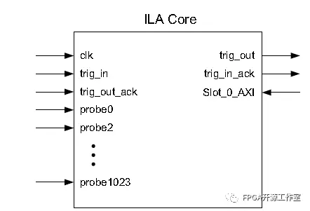
图1 ILA Core
1.2 VIO (Virtual Input/Output core)
VIO核是一个可定制的核,可以实时监控和驱动内部FPGA信号。不像ILA核,不需要片上或片外RAM。
VIO核有两种类型的信号:
. Input probes
.Output probes

图2 VIO Block Diagram
2 ila 和 vio在工程中使用
我们使用uart工程来做示例。
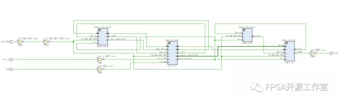
图3 uart示例模块图
如图3所示,整个串口工程包括波特率时钟产生模块,串口接收模块和串口发送模块。我们将使用ila IP对uart_rx模块的接收数据进行debug,使用vio IP对uart_tx模块进行debug。

我们使用Ila将对 rx_data的接收数据进行实时观测,以此来判断程序是否正确。
2.1 ila IP和vio IP的创建
Ila IP的创建,首先打开 IP Catalog如图4。
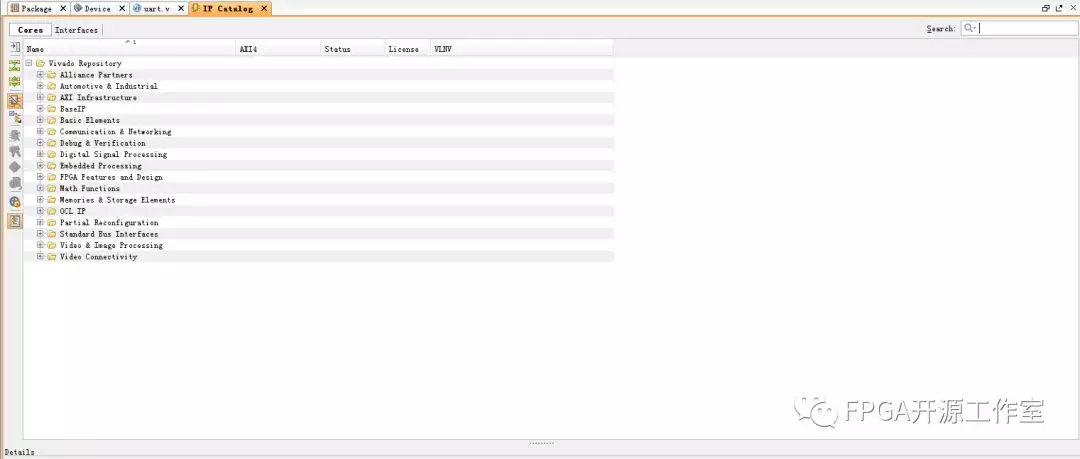
图4 IP Catalog
搜索ila如图5。
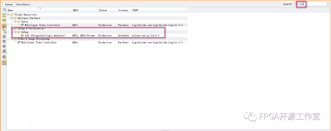
图5 ila ip
双击打开ila IP ,相关参数设置如图6。
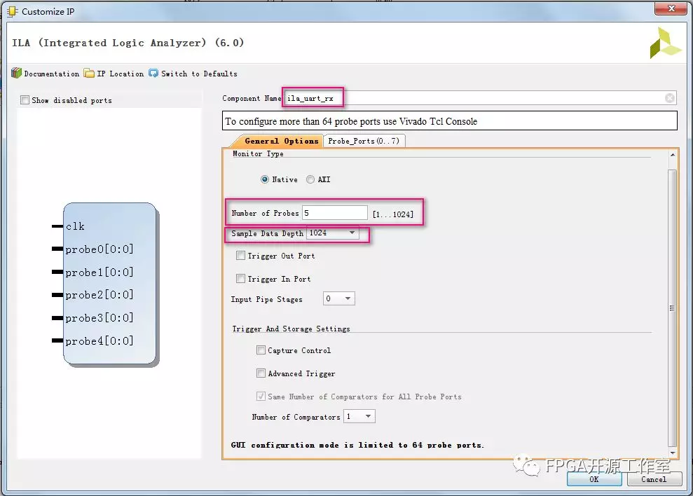
图6 ila IP参数设置
Ila IP的探头位宽设置如图7。
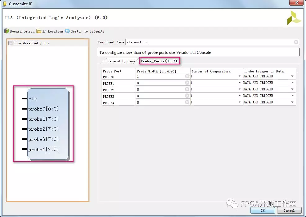
图7 Ila IP位宽的设置
Vio的设置如图8和图9。
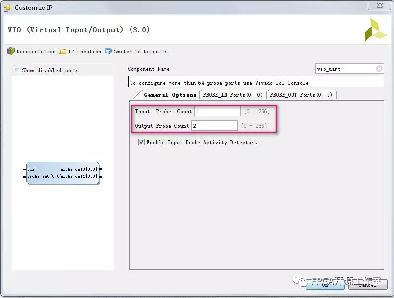
图8 探头个数的设置
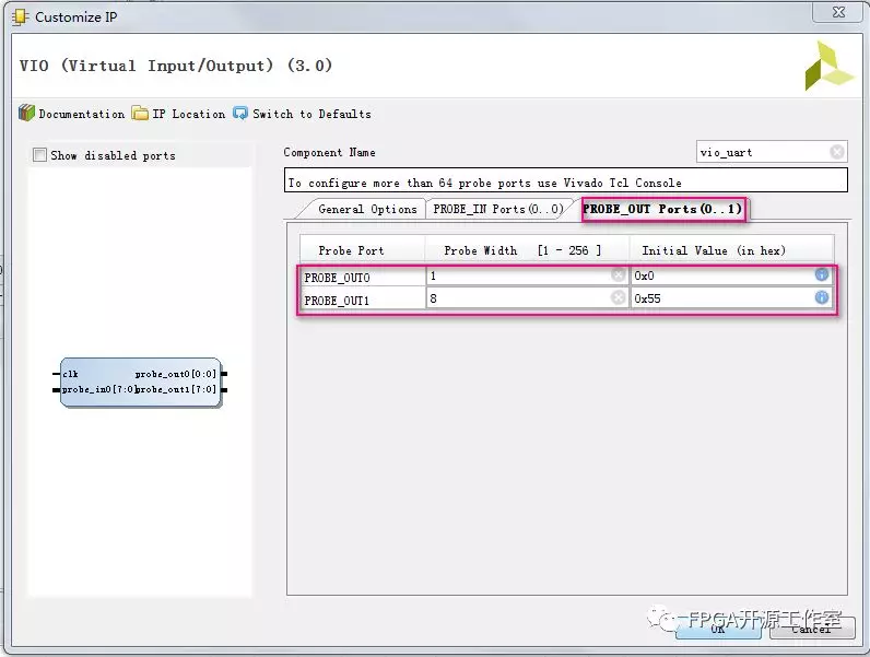
图9 探头数据位宽和初始化值的设置
对Ila IP 和 vio IP的例化。

然后我们综合实现完成后下载程序如图10。

图10 programming FPGA
2.2 ila 和vio对uart的实时数据采集
Ila的调试,我们使用rx_done 信号作为触发信号,设置触发条件等于1,如图11所示。
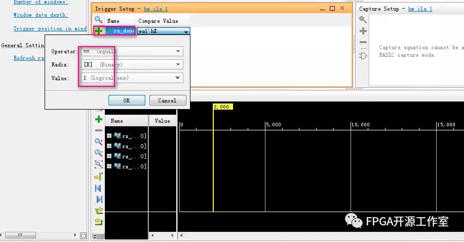
图11 触发条件的设置
我们使用串口工具发送数据,触发以后我们可以观测到FPGA内部rx_data接收完成后的数据如图12。
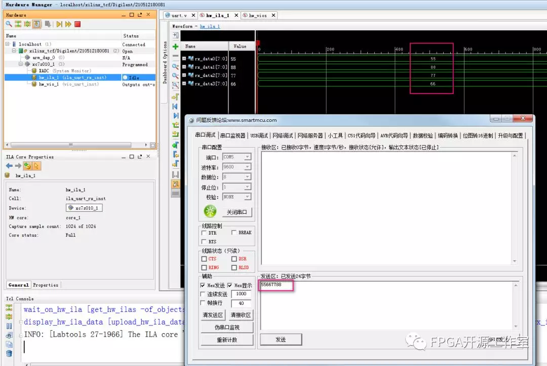
图12 ila IP 观测到FPGA内部信号的变化
Vio的调试,点击+号,添加三个数据端口如图所示13。
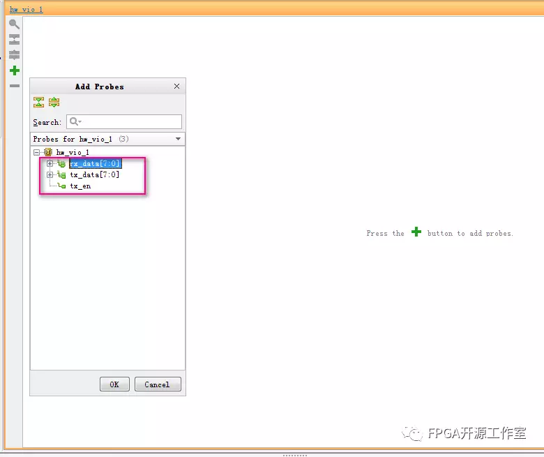
图13 vio观测端口的设置
当tx_en 为1时将tx_data上的数据从FPGA内部发送到串口工具上,如图14所示。
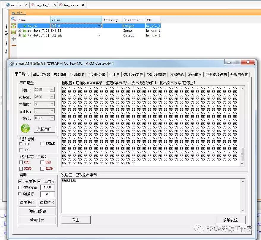
图14 通过vio将数据从FPGA内部发送到串口工具
学会对FPGA内部信号的debug是FPGA设计过程中重要的一环。Vivado的debug相对于ISE更为简单,更加易用。
视频演示:
需要得到本实验原工程的同学可以请联系: FPGA开源工作室
评论
可不可以用VIO中的probe